- 您现在的位置:买卖IC网 > Sheet目录1993 > DS1347T+ (Maxim Integrated Products)IC RTC/CALENDAR SPI 8TDFN
Low-Current, SPI-Compatible
Real-Time Clock
Maxim Integrated
5
DS1347
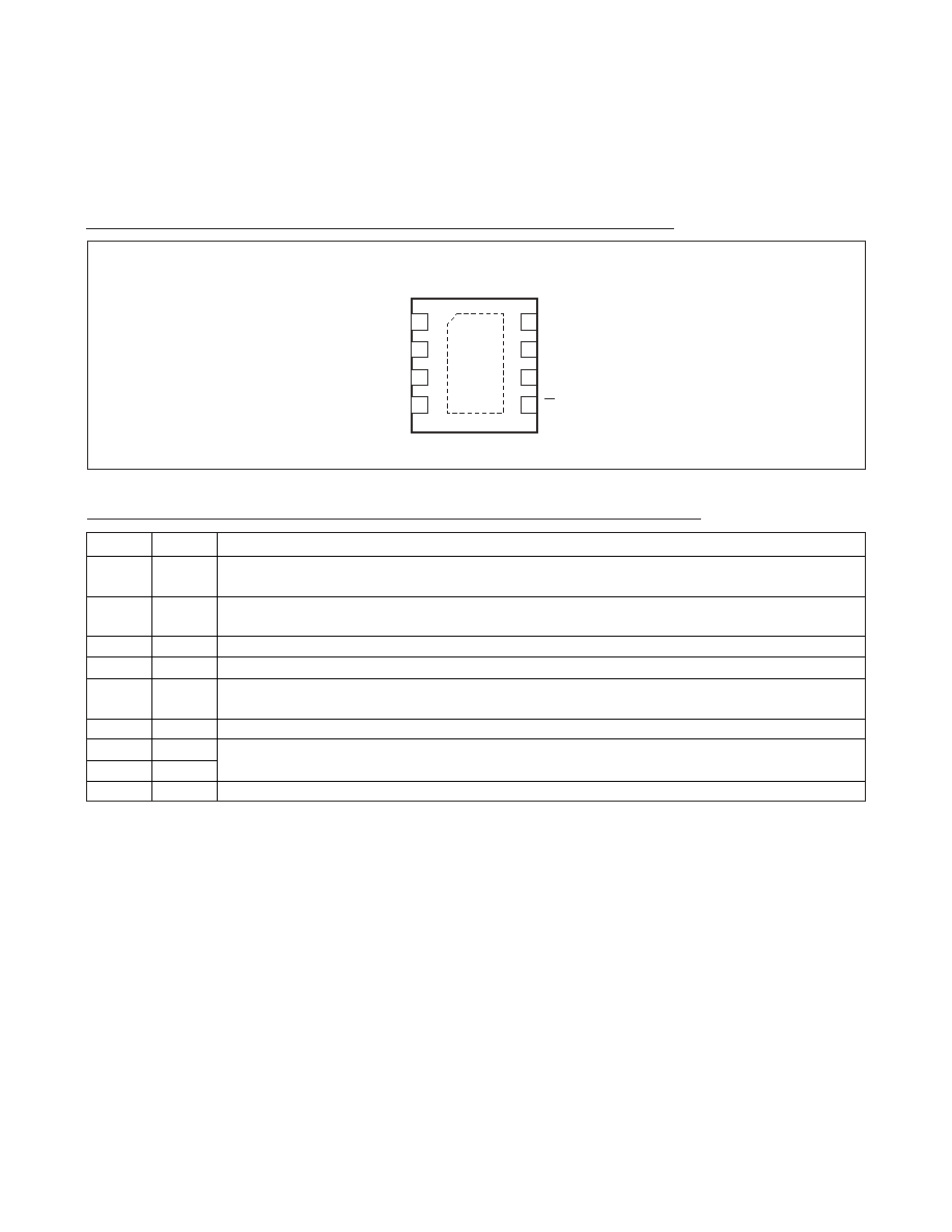
Pin Configuration
VCC
CS
GND
1
2
8
7
X1
X2
DOUT
DIN
SCLK
TDFN
TOP VIEW
3
4
6
5
DS1347
+
EP
Pin Description
PIN
NAME
FUNCTION
1
SCLK
Serial-Clock Input. SCLK is used to synchronize data movement on the serial interface for either 3-wire or
SPI communications.
2
DOUT
Serial-Data Output. When SPI communication is enabled, the DOUT pin is the serial-data output for the SPI
bus.
3
DIN
Serial-Data Input. When SPI communication is enabled, the DIN pin is the serial-data input for the SPI bus.
4
GND
Ground
5
CS
Active-Low Chip Select. The chip-enable signal must be asserted low during a read or a write for SPI
communications.
6
VCC
Power-Supply Input
7
X2
8
X1
Connections for Standard 32.768kHz Quartz Crystal (see the Crystal Characteristics table).
—
EP
Exposed Pad. Connect to GND or leave unconnected.
发布紧急采购,3分钟左右您将得到回复。
相关PDF资料
DS1371U+C01
IC BINARY COUNTER 32-BIT 8-USOP
DS1372U+T&R
IC BINARY COUNTER 32-BIT 8-USOP
DS1374C-3#
IC RTC I2C W/CHARGER 16-SOIC
DS1375T+
IC RTC SERIAL W/ALARM 6-TDFN
DS1384FP-12+
IC CTRLR RTC WDOG 120NS 44-MQFP
DS1386P-8-120+
IC TIMEKEEPER RAM 64K 34-PCM
DS1388Z-3+T&R
IC RTC I2C W/CHARGER 8-SOIC
DS1391U-3+
IC RTC W/CHARGER 10-USOP
相关代理商/技术参数
DS1347T+T&R
制造商:Maxim Integrated Products 功能描述:LOW POWER SPI RTC FOR 12.5PF CRYSTA - Tape and Reel 制造商:Maxim Integrated Products 功能描述:IC RTC/CALENDAR SPI 8TDFN 制造商:Maxim Integrated Products 功能描述:Real Time Clock Low Power SPI RTC For 12.5Pf Crystal
DS1347T+T&R
功能描述:实时时钟 Low Power SPI RTC For 12.5Pf Crystal RoHS:否 制造商:Microchip Technology 功能:Clock, Calendar. Alarm RTC 总线接口:I2C 日期格式:DW:DM:M:Y 时间格式:HH:MM:SS RTC 存储容量:64 B 电源电压-最大:5.5 V 电源电压-最小:1.8 V 最大工作温度:+ 85 C 最小工作温度: 安装风格:Through Hole 封装 / 箱体:PDIP-8 封装:Tube
DS135
制造商:SANYO 制造商全称:Sanyo Semicon Device 功能描述:1.0A Power Rectifier
DS1350AB
制造商:DALLAS 制造商全称:Dallas Semiconductor 功能描述:4096k Nonvolatile SRAM with Battery Monitor
DS1350AB-100
制造商:DALLAS 制造商全称:Dallas Semiconductor 功能描述:4096k Nonvolatile SRAM with Battery Monitor
DS1350AB-70
制造商:DALLAS 制造商全称:Dallas Semiconductor 功能描述:4096k Nonvolatile SRAM with Battery Monitor
DS1350ABL-100
制造商:未知厂家 制造商全称:未知厂家 功能描述:NVRAM (Battery Based)
DS1350ABL-100-IND
制造商:未知厂家 制造商全称:未知厂家 功能描述:NVRAM (Battery Based)